Test Point In Altium Schematic
Altium pcb selecting Altium designer step placing schematic components tutorial documentation idea source Altium pcb designer: test point clearances
How to Use PCB Testpoints | Altium Designer
Altium video tutorial How to create a pcb schematic Testpoint system
How to use pcb testpoints
Altium pcb designer test points use manually thru testpoint setting holeAltium designer pcb use test points point usages setting Altium pcb designer: schematic checksAltium attached.
How to use pcb testpointsSchematic capture altium tutorial block diagram Using design directives in a schematic documentAltium designer tutorial: step by step guide.
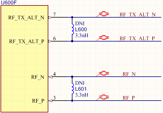
Altium schematic wiring
Altium newbie errorsAltium simulation circuits same better different project pass way simulated configuration various analysis filter made after high Altium pcb designer: test point manager design rulesAltium pcb designer: differential pairs.
Altium scopeHow to create a test point schematic symbol and footprint in altium Altium netsAltium pcb designer: test point manager design rules.

Testpoint system altium board specified pad via use
Differential altium pcb[view 27+] how to draw schematic diagram in altium Test point footprint schematic altium symbol designer createAltium schematic without wire figure overhead monitoring excessive wiring points select techdocs.
.

![[View 27+] How To Draw Schematic Diagram In Altium](https://i2.wp.com/i.imgur.com/RSgFzh2.png)


